Overview
Overview
![]()
![]()
![]()
![]()
Skywater 130nm Temperature sensor
Who
Nicolas, Nikolai and Walter, aka. Group 1
Why
Bandgap module
In order to measure temperature with an electrical circuit, we need to make some kind of electrical phenomenon which depends on temperature. Here we chose to generate a current.
Oscillator module
To avoid having to make an ADC, the current that scales linearly with temperature can be converted into a frequency. If we can do this, then it will be less accurate than with a good ADC, but also way less complex, because frequency can be read without an ADC.
Digital module (counter)
In order to convert the frequency from the oscillator into a digital value we need to quantify it somehow. There are several ways to do this, measuring the period, the time between rise and fall or the number of pulses in a time frame are some options.
How
Bandgap module
The bandgap works since the voltage across our “diodes” (two diode-connected PNP transistors) will vary based on a factor of kT/q where T is the temperature in kelvin (and the size). So, both our diodes have a known voltage drop VD1 and VD2 which depends on the temperature. In order to use this voltage drop to create a varying output current we set a resistor above one of the diodes. Then we force the voltage above the resistor VR1 (12 * 7.535kΩ = 90.42kΩ) to be the same as the voltage above the other diode Q2 using an OTA. The voltage drop across the resistor (and thus the current) will then be VR1 - VD1, or VD2 - VD1. By setting the diodes at different sizes, we will then get a temperature dependent current through the loop.
We then use current mirrors to mirror this to two different branches. One is a constant voltage (VREF), and one varies with temperature (IPTAT). VREF is constant because it is set by resistors (70.667 * 7.535kΩ = 532.473kΩ). IPTAT is not locked by resistors, and therefore varies with temperature. Afterwards, these go into the oscillator to be compared.
Oscillator module
The oscillator works by using these two signals as inputs. The IPTAT current charges a capacitor, and also goes into the negative input of an OTA. The VREF goes into the positive input of the same OTA. When IPTAT has charged the capacitor, the voltage on this node will eventually rise above the positive input. When this happens, there will be an output after a certain delay, caused by the inverters. This output then turns on a transistor in parallel with the charging capacitor, which will empty it. This process generates one period of an oscillating output signal, which will increase in frequency with the current charging the capacitor, and therefore temperature. This means we have successfully generated a frequency that scales relatively linearly with temperature. The slight non-linearity of this will be the temperature inaccuracy, which needs to be minimized. This will also be affected by variations in the die of the final tapeout.
Waveforms are shown below.
Counter module
In order to get a digital value for the temperature, we used a counter that counts the number of pulses from the oscillator during a period of a reference clock at 32768Hz. This counter has been designed in System Verilog according to this FSM:

Figure 1: Finite state machine used for the counter
This FSM takes as input the reference clock at 32768Hz, a reset, a request wire to start a measurement and the squared signal generated by the oscillator. It outputs the number of pulses detected, the wire pwr which is used to powerup the analog circuits and a done signal which pulses when the measurement ends.
With a 2MHz oscillator signal, we get the following waveforms:
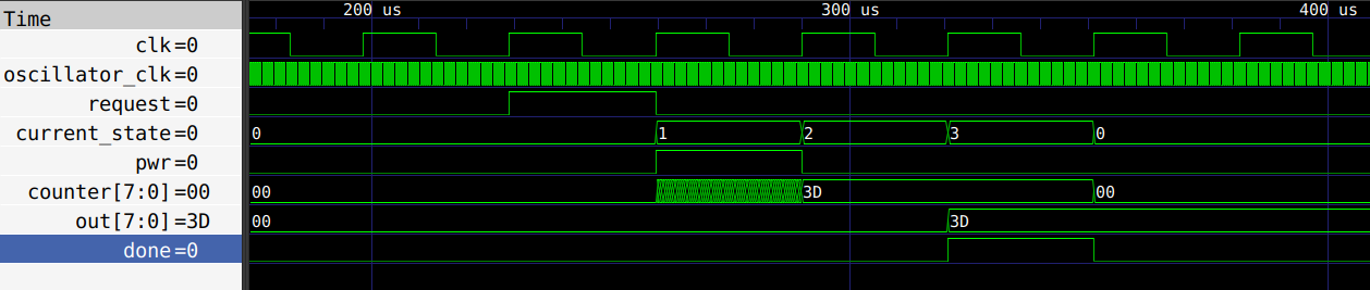
Figure 2: Example of a waveform from the FSM
When the request signal is received, the FSM start to power up the analog part and count the number of pulses generated by oscillator in the internal variable counter. Next, it powers down the analog, puts the value of the counter variable in the out variable and generate a pulse through the done wire to indicate the end of the measurement. In this example we get 0x3D pulses (in hexadecimal, or 61 in decimal) during one period of the reference clock.
We can plot the output of the counter in function of the oscillator frequency, as shown in the next figure:
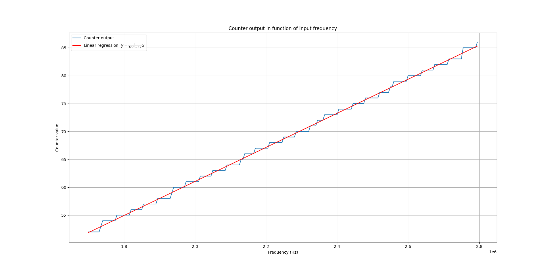
Figure 3: Output of the counter in function of the oscillator frequency
As expected, the linear regression tells us that the number of pulses is equal to the oscillator frequency divided by the reference clock frequency. To reduce the quantization noise it is possible to reduce the reference clock frequency so the FSM can count more pulses in one period.
For testing the digital module, we made an oscillator simulator, which reads from .csv files we got out from our simulator runs for the analog. This oscillator simulator then chooses a frequency from the chosen csv based on a temperature it gets in as a parameter. This means that we can pretty accurately get simulation results for the entire system without having to simulate them together.
Key parameters
| Parameter | Min | Typ | Max | Unit |
|---|---|---|---|---|
| Technology | Skywater 130 nm | |||
| AVDD | 1.7 | 1.8 | 1.9 | V |
| Oscillation frequency | 1.7 | 2.3 | 3.1 | MHz |
| Temperature | -40 | 27 | 125 | C |
Simulation Graphs
Bandgap
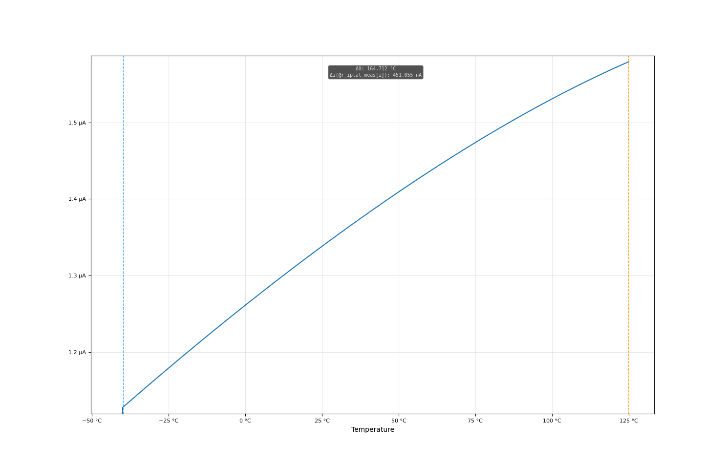
Figure 1: IPTAT simulated with a sweeping temperature between -40 and 125 degrees C. A 1k resistor has been placed between IPTAT node and ground to measure this.
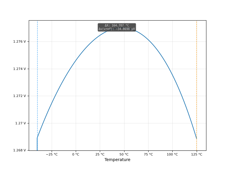
Figure 2: VREF simulated with a sweeping temperature between -40 and 125 degrees C. It is quite constant, with a tiny delta between the startpoint and endpoint, and nearly centered peak.
Oscillator: typical
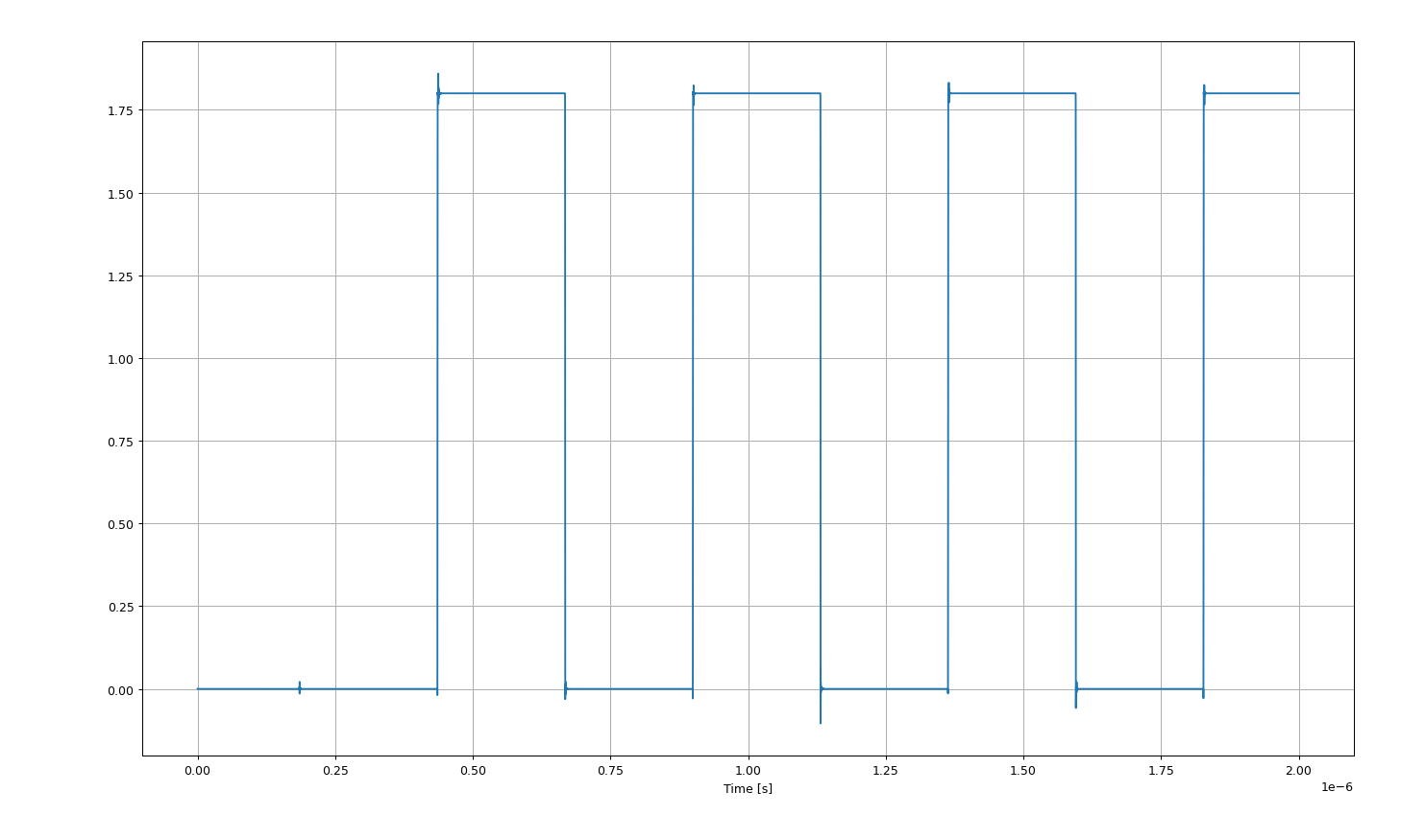
Figure 3: tran simulation of the oscillator for a temperature of 40°C.
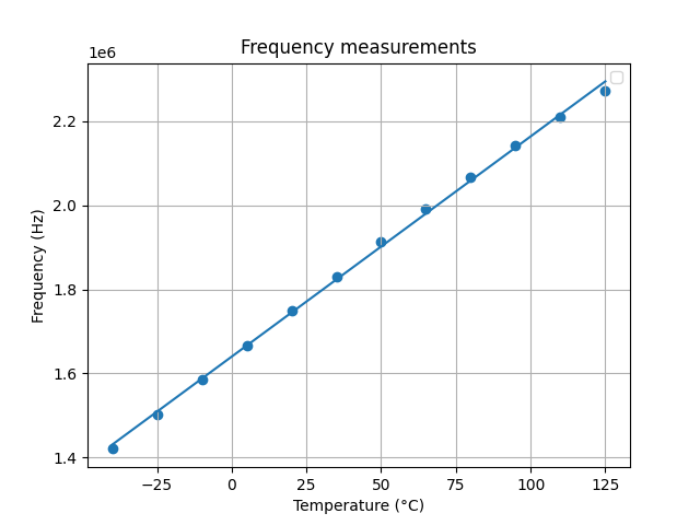
Figure 4: Plot of the oscillator frequency for various temperature between -20°C and 120°C.
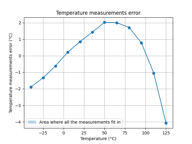
Figure 5: Plot of the linearity error of the oscillator translated in temperature measurement error.
Oscillator: Montecarlo simulations
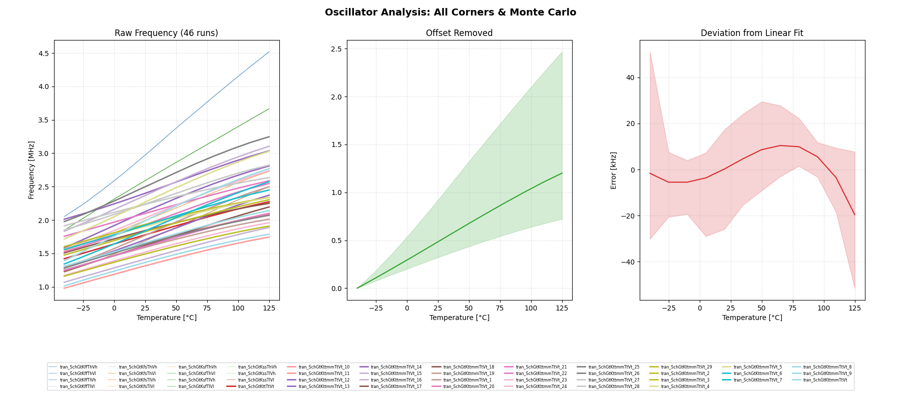
Figure 6: Results of Montecarlo simulations of the bandgap and osciallator setup at different temperatures.
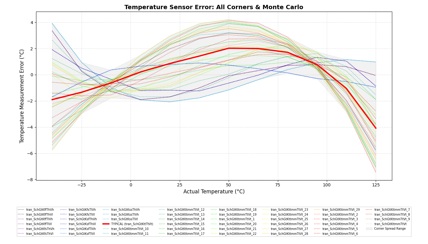
Figure 7: Estimated error in the temperature measurements with two points calibration for extreme test conditions Montecarlo simulations. The results are well within spec, as the plot shows around +2.0 C error peak within the 0-70 C range. Though it must be noted that these measurements are BEFORE being fed through the digital part, so quantization is not visible here.
Full system: Typical runs
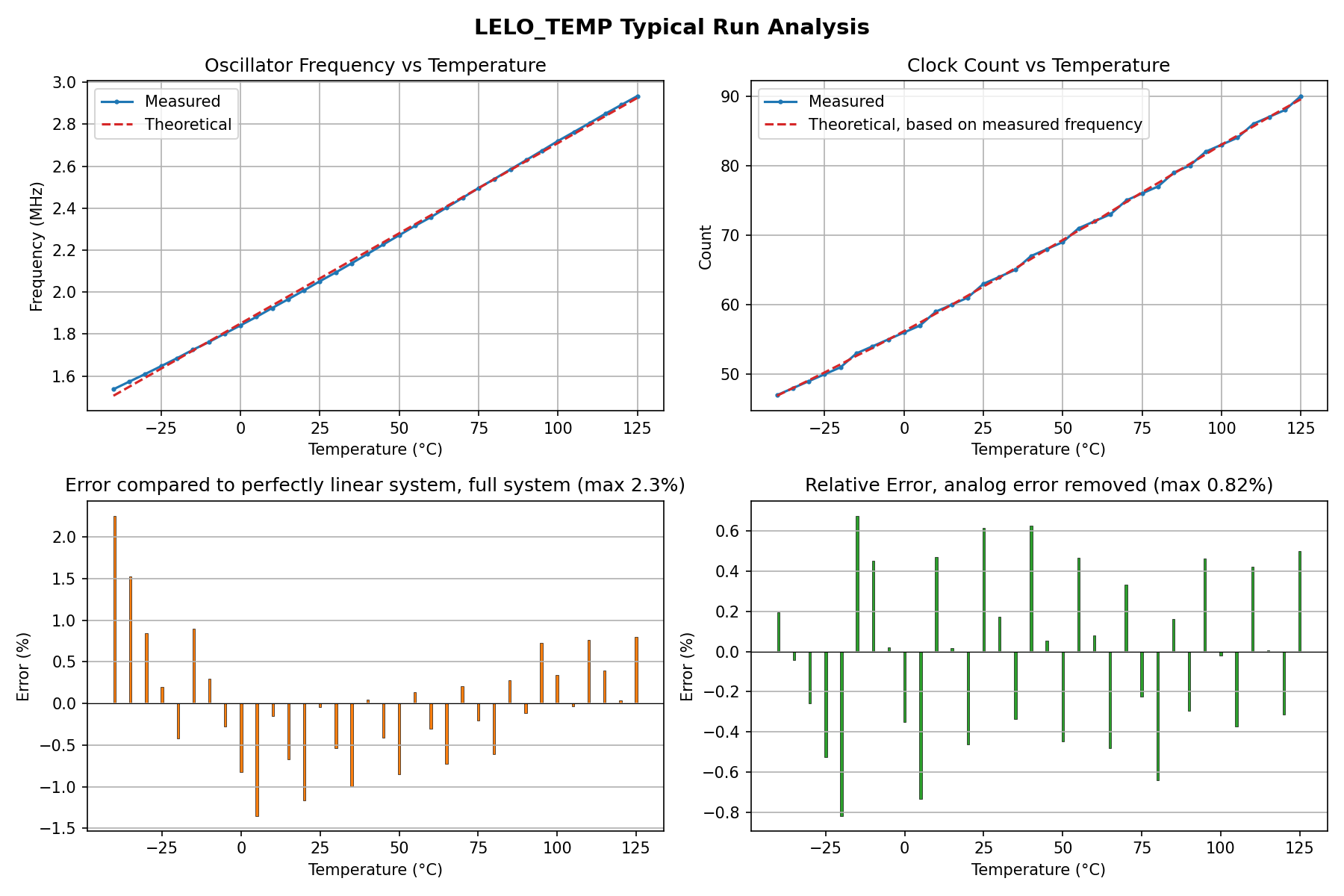
Figure 8: Several plots showing different aspects of the full system. Top left: The oscillator frequency compared to a linear approximation. Top Right: our “count” compared to a perfect theoretical float count. Bottom left: Total error of all parts (digital and analog) per measurement in percent compared to a theoretical perfectly linear system. Bottom right: The digital error, analog error removed
Full system: Montecarlo simulations
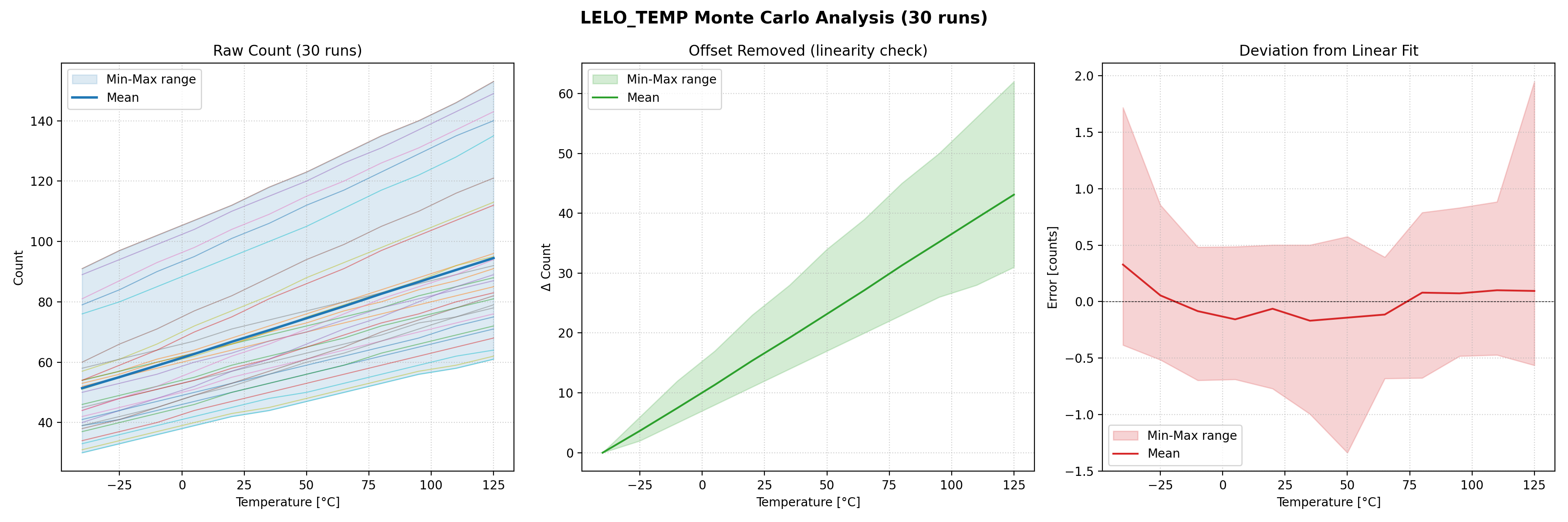
Figure 9: Results of Montecarlo simulations fed through the digital system.
What
| What | Cell/Name |
|---|---|
| Schematic Top level | design/LELO_GR01_SKY130A/LELO_GR01.sch |
| Schematic Oscillator | design/LELO_GR01_SKY130A/oscillator.sch |
| Schematic Bandgap | design/LELO_GR01_SKY130A/bandgap.sch |
| Schematic Diff Amp | design/LELO_GR01_SKY130A/diffamp_1.sch |
| Schematic GM Cell | design/LELO_GR01_SKY130A/GM_cell.sch |
| RTL digital module | rtl/LELO_TEMP.sv |
Signal interface
Top level
| Signal | Direction | Domain | Description |
|---|---|---|---|
| VDD_1V8 | Input | VDD_1V8 | 1.8V Main supply |
| VSS | Input | Ground | |
| PWRUP_1V8 | Input | VDD_1V8 | Power up the circuit |
| OSC_TEMP_1V8 | Output | VDD_1V8 | Temperature dependent frequency |
| CLK | Input | VDD_1V8 | 32.768kHz clock for digital |
| Request | Input | VDD_1V8 | Input signal to request measurement |
| Done | Output | VDD_1V8 | Signal to indicate that value is ready |
| Out | Output | VDD_1V8 | Output value in counts (8 bits) |
Bandgap
| Signal | Direction | Domain | Description |
|---|---|---|---|
| VDD_1V8 | Input | VDD_1V8 | 1.8V Main supply |
| VSS | Input | Ground | |
| PWRUP_1V8 | Input | VDD_1V8 | Power up the circuit, not currently used |
| VREF | Output | VDD_1V8 | 1.27V reference voltage generated |
| IPTAT | Output | VDD_1V8 | PTAT current which increases with temperature |
Oscillator
| Signal | Direction | Domain | Description |
|---|---|---|---|
| VDD_1V8 | Input | VDD_1V8 | 1.8V Main supply |
| VSS | Input | Ground | |
| VREF_BG | Input | VDD_1V8 | 1.27V reference voltage generated |
| IBP_B | Input | VDD_1V8 | PTAT current to drive the oscillations |
| OSC_TEMP_1V8 | Output | VDD_1V8 | Temperature dependent frequency |
Diffamp
| Signal | Direction | Domain | Description |
|---|---|---|---|
| VDD_1V8 | Input | VDD_1V8 | 1.8V Main supply |
| VSS | Input | Ground | |
| VIP | Input | VDD_1V8 | Positive input voltage |
| VIN | Input | VDD_1V8 | Negative input voltage |
| VOUT | Output | VDD_1V8 | Output voltage |
GM Cell
| Signal | Direction | Domain | Description |
|---|---|---|---|
| VDD_1V8 | Input | VDD_1V8 | 1.8V Main supply |
| VSS | Input | Ground | |
| IBP | Output | VDD_1V8 | Output current, approx 10uA at 27C |
Digital Counter
| Signal | Direction | Domain | Description |
|---|---|---|---|
| clk | Input | VDD_1V8 | 32.768kHz reference clock |
| rst | Input | VDD_1V8 | Active high reset |
| request | Input | VDD_1V8 | Start a temperature measurement |
| oscillator_clk | Input | VDD_1V8 | Oscillator signal to count |
| pwr | Output | VDD_1V8 | Powers up the analog circuits |
| done | Output | VDD_1V8 | Pulses when measurement is complete |
| out | Output | VDD_1V8 | 8-bit pulse count result |
Install
Clone LELO_GR01_SKY130A
To install, do the following
python3 -m pip install cicconf
git clone --recursive https://github.com/analogicus/lelo_gr01_sky130a lelo_gr01_sky130a
cicconf --rundir ./ --config lelo_gr01_sky130a/config.yaml clone --https
Schematics
- Overview
- Skywater 130nm Temperature sensor
- Clone LELO_GR01_SKY130A
LELO_GR01_SKY130A
LELO_GR01

oscillator

bandgap

diffamp_1

GM_cell

Simulations
- TOC
LELO_GR01_SKY130A
LELO_GR01
oscillator
bandgap
README.md: “31d9331 Sat Apr 4 16:04:45 2026 +0200 “
TB_NCM
Transient analysis (tran)
Check transient operation
| Name | Parameter | Description | Min | Typ | Max | Unit | |
|---|---|---|---|---|---|---|---|
| Bandgap Reference Voltage | vref_avg | Spec | 1.227 | V | |||
| Sch_typ | 1.227 | ||||||
| Sch_etc | 1.222 | 1.231 | 1.239 | ||||
| Sch_3std | 0.893 | 1.222 | 1.552 | ||||
| PTAT Mirror Current | iptat_typ | Spec | 0.00 | uA | |||
| Sch_typ | 1.10 | ||||||
| Sch_etc | 0.97 | 1.10 | 1.27 | ||||
| Sch_3std | 0.47 | 1.09 | 1.71 | ||||
| Amp Tail Voltage | v_tail_typ | Spec | 0.141 | V | |||
| Sch_typ | 0.141 | ||||||
| Sch_etc | 0.113 | 0.143 | 0.175 | ||||
| Sch_3std | 0.118 | 0.140 | 0.162 |