![]()
![]()
![]()
![]()
![]()
Who
Reidar Arne Eidsvik Nerheim, Pol Batalle Largo and Tord Olsen Sætermo.
Why
This project is a part of the course “TFE4188 - Advanced Integrated Circuits” at NTNU during the spring of 2025.
How
We used tools such as xschem, ngspice, and magic.
What
| What | Cell/Name |
|---|---|
| Schematic | design/JNW_GR07_SKY130A/amplifier.sch |
| Layout | design/JNW_GR07_SKY130A/amplifier.mag |
| Schematic | design/JNW_GR07_SKY130A/temp_to_current.sch |
| Layout | design/JNW_GR07_SKY130A/temp_to_current.mag |
| Schematic | design/JNW_GR07_SKY130A/JNW_GR07.sch |
| Layout | design/JNW_GR07_SKY130A/JNW_GR07.mag |
Changelog/Plan
| Version | Status | Comment |
|---|---|---|
| 0.1.0 | Milestone 0: Sim setup | |
| 0.1.1 | Milestone 1: Current PTAT | |
| 0.1.2 | Milestone 2: Digital output | |
| 0.1.3 | Simulate circuit at different corners | |
| 0.1.4 | Simulate circuit at different supply voltages | |
| 0.1.5 | Milestone 3: Layout |
Signal interface
| Signal | Direction | Domain | Description |
|---|---|---|---|
| VDD | Input | VDD_1V8 | Main supply |
| VSS | Input | Ground | |
| CLK | Input | Clock | Clock signal |
| PWM | Output | Digital | Digital output signal proportional to temperature |
Key parameters
| Parameter | Min | Typ | Max | Unit |
|---|---|---|---|---|
| Technology | Skywater 130 nm | |||
| AVDD | 1.7 | 1.8 | 1.9 | V |
| Temperature | -40 | 27 | 120 | C |
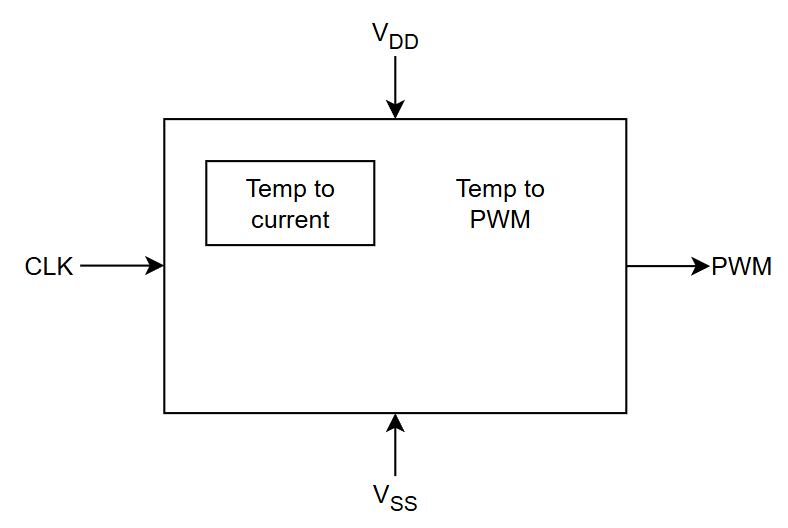
System description
This is a temperature measurement circuit. It is built up of two blocks:
- Temp to Current, a circuit that outputs a current proportional to absolute temperature (PTAT)
- Current to PWM, a circuit that outputs a digital PWM signal proportional to temperature
The system is depicted below
Temperature to Current, PTAT
Aka Milestone 1
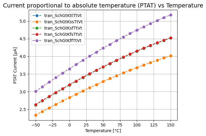
The PTAT circuit can be found in “design/JNW_GR07_SKY130A/temp_to_current.sch”, and is shown in the figure below.
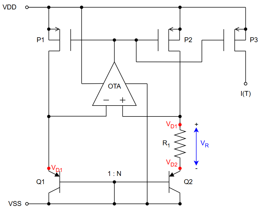
The circuit exploits the temperature (T) dependency and size difference (N) of diode 1 and diode 2 to create a current I(T) dependent on temperature. The voltage over diode 1 is $V_{D1} = V_T ln\frac{I_D}{I_{S1}}$, and the voltage over diode 2 is $V_{D2} = V_T ln\frac{I_D}{I_{S2}}$. Assuming that the opamp is ideal, the voltage on it’s negative input is set equal to it’s positive input, meaning $V_{D1} = V^- = V^+$. This creates a voltage drop accross the resistor $R_1$ of $V_{R_1} = V_{D1} - V_{D2} = V_T ln\frac{I_{S2}}{I_{S1}}$. Since diode 2 is N times larger than diode 1, we can assume $I_{S2} \approx N I_{S1}$, meaning that $V_{R_1}$ can be simplified to $V_{R_1} \approx V_T ln(N)$. The current through $R_1$ is then $I_{R_1} = \frac{V_{R_1}}{R_1} = \frac{V_t}{R_1} ln (N)$. Since $V_T = \frac{kT}{q}$, we get a current proportional to temperature: $I_{R_1}(T) = \frac{kT}{qR_1} ln(N)$. This current is copied using a current mirror, creating $I(T)$ and used as an output.
Note: Diode 1 and diode 2 are realized by the NPN transistors Q1 and Q2 respectivly.
Testing of the PTAT circuit
To test the circuit follow these steps: <!–
- enter directory “jnw_gr07_sky130a/sim/temp_to_current_tb “
- run “make typical”. This will sweep the temperature in the range -40 to 130 degrees celcius
-
To see results run “cicsim wave output/tran_SchGtKttTtVt.raw” and plot the current “i(v.xdut.v1)”. –>
- enter directory “sim/temperature_to_current_tord/”
- run “make typical” or some other make command as specified in the Makefile. This will simulate the circuit at temperatures from -30 to 130 degrees celcius.
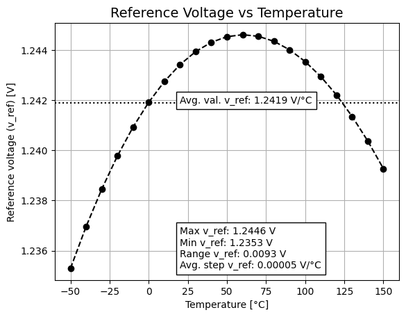
- The make typical simulations results in the plots seen below. The plots are saved as plots/ptat_vs_temp_SchGtKttTtVt.png and plots/vref_vs_temp_SchGtKttTtVt.png.
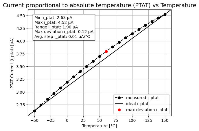
The plots of ptat current from other simulations (for example corners) can be seen by running the python file plot_ptat.py with the yaml file(s) location in the folder “output_tran/” as arguments, ex: python plot_ptat.py output_tran/tran_SchGtKttTtVt output_tran/tran_SchGtKffTtVt output_tran/tran_SchGtKssTtVt output_tran/tran_SchGtKsfTtVt output_tran/tran_SchGtKfsTtVt. This will save the plot as plots/ptat_vs_temp.png
Current to PWM (JNW_GR07)
Aka Milestone 2
The current to PWM circuit can be found in “design/JNW_GR07_SKY130A/temp_to_pwm_RA.sch”, and is shown in the figure below.
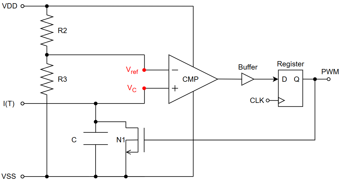
The circuit used the input current $I(T)$ to charge a capacitor. The voltage across the capacitor is used as input voltage of the positive node of a comparator, $V^+ = V_C$. The negative node is connected to a reference voltage $V^- = V_{ref}$, created by a voltage divider consisting of two resistors, $R_2$ and $R_3$. This gives $V^- = V_{ref}= V_{DD} \frac{R_3}{R_3+R_2}$. The voltage across the capacitor can be approximated as $V_C(t) = V^+ = \int_{0}^{t} \frac{I(T)}{C} \ dt \approx \frac{tI(T)}{C}$, assuming that
- $V_C(t=0) = 0$, the voltage starts at 0 when time is 0.
- $\frac{\partial T}{\partial t} = 0$, the temperature is not dependent on time.
The oputput of the comparator is set to high at time $t_0$, when $V^- = V^+(t_0)$. Using the previous equations this can be written as $V_{ref} = \frac{t_0I(T)}{C}$. The time $t_0$ is thus given by $t_0 = \frac{V_{ref}C}{I(t)}$. The output of the comparator is buffered, then fed into a clocked register. The output of the register is the PWM signal, and is simultaneously used to reset the circuit. The reset is done by discharging the capacitor using an nmos, N1, connected to ground.
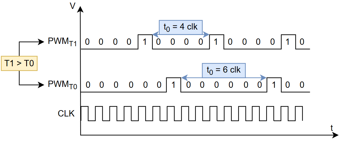
It can be shown using previous formulas (found in section “Temp to Current, PTAT”), that $\frac{\partial I(T)}{\partial T} > 0$, meaning that a higher T results in lower $t_0$. This means that higher temperatures results in a PWM signal with higher mean voltage (RMS). This is depicted the figure below, where temperature $T1 > T0$.
Testing of the PWM circuit
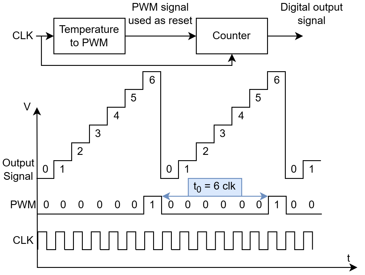
In order to extract $t_0$, the PWM circuit is used to control a 8-bit digital counter during testing. The counter will continously count upwards, reseting when PWM goes high. The value of the counter when reset is set high is then linearly dependent on temperature. The test circuit is depicted in the figure below.
To run simulations follow these steps:
- enter directory /sim/temp_to_pwm_RA
- type “make typical”. This will simulate the circuit using the digital circuit found in “digital.so” (compiled using “digital.v”), the testbench in “tran.spi”, and the “tran.meas” file. (Note that simulating takes a lot of time since it runs across multiple temperatures!)
- plot the output using “plot.py” => “python plot.py output_tran/{…}.yaml”
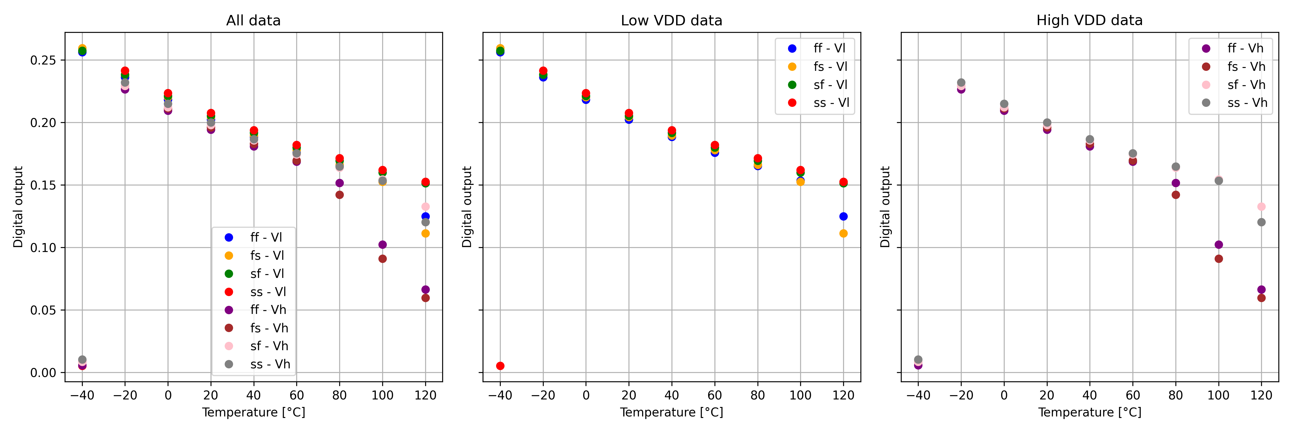
- the plot is saved as “plot.png”, and is depicted below.
Note that the digital output is expressed as a float value, explaining the magnitude of the y-axis. Also, the sudden drop at 120 degrees will be looked into :) (althoug since this is a unique digital value, it would not cause problems in a digital circuit…)
Note:
- There also exists a simple testbench, “design/JNW_GR07_SKY130A/temp_to_pwm_RA_TB.sch”, that can be used for initial simulations of the circuit.
- The temperature to current block used for the PWM circuit can be found in “desin/JNW_GR07_SKY130A/temp_to_current.sch”, and is not sized identical to the one tested in chapter Temp to current, PTAT.
Layout of PWM circuit (JNW_GR07.mag)
Aka Milestone 3
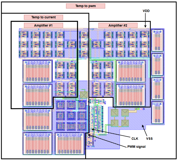
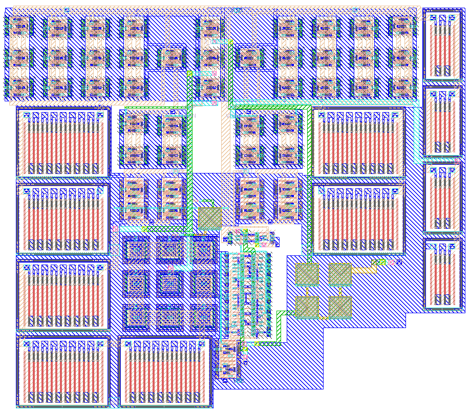
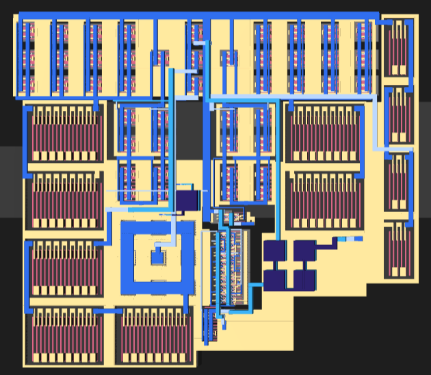
The layout of the PWM circuit can be found in “design/JNW_GR07_SKY130A/JNW_GR07.mag”, and is depicted below (both with / without explanation, and a 3d render). Layout vs schematic (LVS) can be tested by running “make cdl lvs” in the work folder. The layout succesfully completes the LVS test, and does not experience any design rule errors (succesfully completes the drc, design rule check).
Note Ther are two revisions of the layout, this being revision 2. The components are: “amplifier_rev2.mag” and “temp_to_current_rev2.mag”.
Layout with explanation:
Layout without explanation:
3d render of layout:
Future Work
Although the layout succesfully completes the tests, it needs refinement:
- Do layout simulations.
- Insert dummy components in order to reduce mismatch.
- Current should run in the same direction for components that should match.
- The circuit could probably be made smaller.
OTA
The amplifier in the PTAT circuit and the comparator in the PWM circuit is both realized by identical OTA’s. The OTA can be found in “design/JNW_GR07_SKY130A/amplifier.sch”. The OTA is a differential input, single stage transducer. A simple testbench can be found in “design/JNW_GR07_SKY130A/amplifier_tb.sch”.